CoWoS is the constraint on AI accelerator supply, and the constraint inside CoWoS is materials rather than tools. Chip-on-Wafer-on-Substrate mounts logic and HBM dies on a silicon interposer and mounts that interposer on an organic substrate. Building one takes twelve distinct material classes, and more than 90% of them come from Japanese suppliers, several of whom hold an effective monopoly on a single formulation.
That arrangement is efficient at steady volume and fragile during a ramp. It is also why the interesting question for a validation team is no longer which node a part is on. It is which materials the part is qualified against, and what happens to the test plan when one of them has to change.
A CoWoS package is not glued together, it is formulated
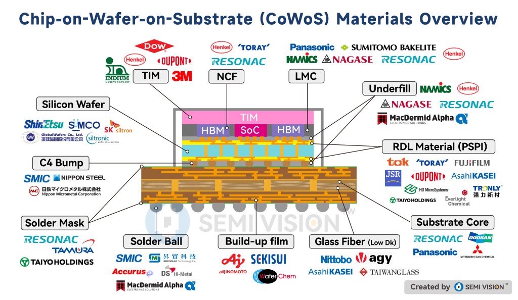
The mental model most people carry is that advanced packaging is assembly: dies go on an interposer, the interposer goes on a substrate, done. The assembly is the easy part. Every interface in Fig. 1 is a chemistry with its own supplier list, its own qualification history, and its own failure mode.
Four of those chemistries carry most of the risk, because each one is both performance-critical and concentrated.
Redistribution layers
The routing that makes an interposer worth having. It depends on high-purity photosensitive polyimide, and the resolution of the finished trace is a property of the resin, not only of the lithography.
Underfill and TIMs
Underfill keeps the microbump joints intact through thermal cycling, and the thermal interface material is what stops a 700W package cooking itself. Both are the difference between a part that works and a part that works for three years.
Advanced substrates
The ABF build-up film shortage of 2021 is the precedent. One dielectric film, one dominant supplier, and finished silicon sitting in a warehouse waiting for a substrate to mount it on.
Solder balls and bumps
Microbump pitch is now measured in single-digit microns. At that size the impurity budget of the solder alloy stops being a specification and starts being the yield.
None of this is exotic on its own. What makes it a bottleneck is that all twelve classes have to be qualified together, as one package, against one reliability standard. Change any of them and the qualification is not partially valid. It is open again.
The 90% factor
Here is the part that gets underestimated. More than 90% of the backend materials used in CoWoS come from Japanese suppliers. Resonac, Ajinomoto, Shin-Etsu, JSR, TOK, and Toray between them hold near-monopolies on specific chemical formulations that nobody else has qualified at volume.
That concentration is not an accident and it is not incompetence elsewhere. These are decades-old specialty chemical positions, protected by process knowledge that does not transfer with a licence. It worked well when packaging volumes were steady and predictable. It is a different proposition when accelerator demand asks the same suppliers to double output inside a year.
A fab can be financed. A specialty chemical position that took twenty years to build cannot be financed into existence in twelve months.
The early signal is already visible in the OSAT ecosystem, where material allocation, not tool availability, is what moves a build date. Read that alongside the wider AI chip supply chain monopoly and the pattern is consistent: the scarce asset is never the one with the biggest capex number attached to it.
Twelve material classes, one package
The table below is the bill of materials behind Fig. 1, layer by layer, with the suppliers named on the reference diagram that follows it. The right-hand column is where the named suppliers are headquartered, not a market share.
| Layer | What it does | Named suppliers | Supply base |
|---|---|---|---|
| TIM | Moves heat from the die into the lid | Indium, Henkel, Dow, DuPont, 3M | US + JP |
| NCF | Non-conductive film bonding stacked dies | Henkel, Toray, Resonac | JP |
| LMC | Liquid molding compound over the assembly | Panasonic, Sumitomo Bakelite, Namics, Nagase, Resonac | JP |
| Underfill | Fills the microbump gap so the joints survive thermal cycling | Namics, Henkel, Nagase, Resonac, MacDermid Alpha | JP |
| RDL (PSPI) | Photosensitive polyimide that defines the routing on the interposer | TOK, Toray, Fujifilm, JSR, DuPont, Asahi Kasei, HD MicroSystems, Taiyo Holdings | JP |
| Silicon wafer | The interposer itself | Shin-Etsu, SUMCO, GlobalWafers, SK Siltron, Siltronic | JP + TW + KR |
| C4 bump | Connects interposer down to substrate | Nippon Steel, Nippon Micrometal | JP |
| Substrate core | The stiff middle the package is built out from | Resonac, Doosan, Panasonic, Mitsubishi Gas Chemical | JP + KR |
| Build-up film | ABF dielectric laminations either side of the core | Ajinomoto, Sekisui | JP |
| Glass fiber | Low-Dk woven cloth inside the core | Nittobo, AGY, Asahi Kasei, Taiwan Glass | JP + TW + US |
| Solder ball | Connects the package down to the board | Shenmao, Accurus, DS Hi-Metal, MacDermid Alpha | TW + KR + US |
| Solder mask | The protective skin over the substrate | Resonac, Tamura, Taiyo Holdings | JP |
Count the Japanese entries. Then note that several names appear on four or five rows: Resonac alone shows up in the NCF, molding compound, underfill, substrate core, and solder mask lines. A single supplier disruption is not a single-layer problem.
The requalification scramble
When a primary material runs short, OSATs race to qualify a second source. That race is where the supply chain problem becomes a validation problem.
Requalification does not shorten under pressure
Swapping a single underfill means thermal cycling, highly accelerated stress testing, and electromigration validation before anything ships. The failure being tested for is delamination or a cracked joint that surfaces after months in the field, so the test has to run long enough to find it. Commercial urgency does not compress that clock, it only raises the cost of getting it wrong.
Materials interact, and the interactions are the hard part
A replacement TIM can behave differently against the lid than against the die, and a new underfill can change how the package moves through reflow. The qualification is of the combination, not the component, which is why a two-material substitution is not twice the work of a one-material substitution. It is a new matrix.
The data burden lands on the bench
Each of those runs produces long, repetitive, instrument-driven sequences and a lot of measured data that has to survive an audit. Teams still running that on hand-maintained spreadsheets and one engineer's LabVIEW code discover the real cost of a second source at exactly the moment they can least afford it. Our guide to automating test reports covers the data model that makes this generatable rather than manual.
What a materials constraint looks like from the lab
If you run reliability or package validation, the supply chain story arrives as three concrete changes to your week.
- More runs, same headcount. A second source is a full qualification matrix, and it lands on top of the schedule you already had, not instead of it.
- Longer sequences with unattended time. Thermal cycling and HAST run for days. Anything that needs a human to advance a step is where the schedule leaks.
- Evidence that has to hold up. A requalification report is read by a customer's quality organisation. Measured values, bounds, and verdicts have to trace back to the run that produced them.
That last point is the one most labs underestimate. The bottleneck in a requalification is rarely the instrument time. It is the authoring, the babysitting, and the reporting around it, which is the same argument behind comparing test automation software honestly rather than defaulting to whatever the last engineer wrote in.
Advanced packaging is the new battleground
The shift is quiet but unmistakable. Advanced packaging has stopped being a supporting function of the semiconductor industry and started being the competitive position. CoWoS is not a die-stacking technique. It is a claim on a materials ecosystem, and what TSMC is doing next with System-on-Wafer extends that claim rather than replacing it.
We still talk about nodes, because nodes are legible and have numbers on them. The leverage moved downstream. The companies that secure ABF substrates, specialised underfills, and high-purity solder are the ones that actually ship parts, and the packaging ecosystem map is now a more useful read of the industry than a roadmap of nodes.
For everyone downstream of that, including the engineers who have to prove a substituted material is safe, the practical consequence is simple. Validation throughput is now part of supply chain resilience. Read 2.5D versus 3D and the chiplet value chain for where this goes next.
Questions engineers ask about CoWoS
What is CoWoS packaging?
CoWoS stands for Chip-on-Wafer-on-Substrate. It is TSMC’s 2.5D advanced packaging process: logic and HBM dies are mounted on a silicon interposer (the wafer), and that interposer is mounted on an organic substrate. The interposer carries redistribution layers dense enough to connect an SoC to its memory stacks at a bandwidth a conventional substrate cannot reach.
Why is CoWoS the bottleneck for AI chips rather than the silicon?
Every high-bandwidth AI accelerator needs an interposer and HBM stacks, so no accelerator ships without a CoWoS slot. Front-end wafer capacity can be added at a different node or a different fab, but the backend line and the materials feeding it cannot be substituted the same way. The constraint moved downstream.
Which companies supply CoWoS materials?
Twelve material classes go into one package, and the named suppliers are concentrated in Japan: Resonac, Ajinomoto, Shin-Etsu, JSR, TOK, Toray, Fujifilm, Asahi Kasei, Namics, Nagase, Sumitomo Bakelite, Panasonic, Nittobo, Sekisui, Taiyo Holdings, Nippon Steel, and Mitsubishi Gas Chemical, alongside Henkel, Dow, DuPont, 3M, Indium, and MacDermid Alpha outside it.
How much of the CoWoS material supply comes from Japan?
More than 90% of the backend materials used in CoWoS come from Japanese suppliers. Several of them hold effective near-monopolies on a single chemical formulation, which is a workable arrangement at steady volume and a fragile one during a ramp.
What happens when a packaging material is second-sourced?
The package has to be requalified. A replacement underfill or TIM goes through thermal cycling, highly accelerated stress testing, and electromigration validation before it can ship, because the failure it can introduce is delamination or a cracked joint that only appears after months in the field. That work is measured in months, not weeks.
Is the CoWoS constraint about capacity or about materials?
Both, and they are the same problem seen from two ends. Adding a bonder is a capital decision with a lead time. Adding a qualified second source for a photosensitive polyimide is a chemistry and reliability problem, and no amount of capital shortens the reliability clock.